- ICs
- Magnet
- MicroControllers
- PCB & Solder
-
Small Components
- Aluminium Heat Sink
- Capacitor
- Crystal
- Diodes
- Diodes and Rectifiers
- Fuse
- Fuse Fuse Holder
- General Diodes
- General Purpose Transistor
- Hardware Parts
- Heat Shrink
- Heat Shrink Tube
- Heat Sink
- IC Base Socket
- IC Base ZIF Sockets
- IGBT
- Inductor
- JFET
- LED
- MOSFET
- MOV Metal Oxide Varistor
- Operational Amplifier
- Optocoupler
- PCB Adapter
- Potentiometer
- Power Transistor
- PVC Heat Shrink
- Resistance
- Resistor
- Schottky Diode
- SCR Thyristor
- SMD Resistor Reel
- Speaker
- Splices
- Testing Instruments
- Thermistor
- Transistors
- TRIAC
- Triac Mosfet
- Zener Diode
- SMD Components
- Switches
- AC DC Board Adaptor
- Adapter
-
Battery
- Battery Chargers
- Battery Connector
- Battery Harness
- Battery Holder
- Battery Holder
- Battery Protection Board
- BMS
- Bonka Lipo Battery
- Button Cell Battery
- CNC and PLC Machine Battery
- Coin Cell Battery
- Hearing Aid Battery
- Lead Acid Battery
- Li Ion Battery
- Lipo Battery
- Mobile Battery
- Ni Mh Battery
- Ni-Cd Battery
- Non Rechargeable Battery
- Other Battery Products
- Rechargeable Battery
- Ultra Lithium Battery
- Buck Boost Converter
- Cooling Block
- Cooling Fan
- HI Link Converter
- Meanwell SMPS
- Mornsun Power Supply
- Power Supply Module
- Shavison SMPS & PowerSupply
- SMPS
- Solar Panel
- Transformer
- Voltage Regulators
- 3D Printer Couplings
- 3D Printer Display Controller
- 3D Printer Extruder Kit
- 3D Printer Extruder Part And Fan
- 3D Printer Heat Bed Accessories
- 3D Printer Nozzle
- 3D Printer Parts
- 3D Printing Pen
- Basic Robot Parts
- DC Motor
- DIY STEM Kit
- Drone
- Drone Parts
- Lead Screw and Nut
- Motor Accessories
- Motor Driver
- Motor Driver IC
- New Arrival
- Home
- Electronic Components
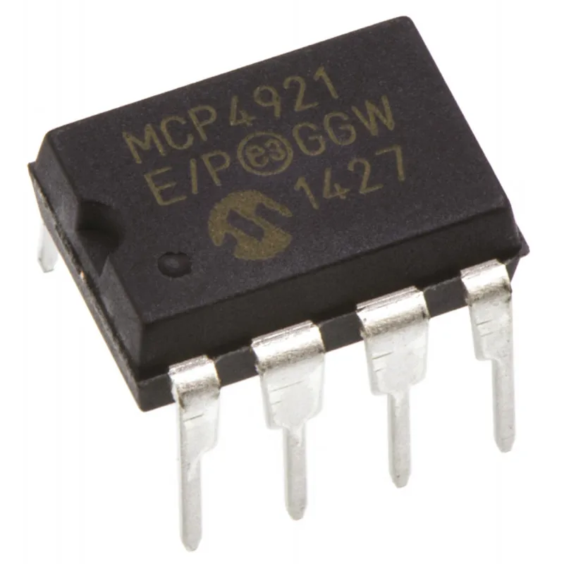
- MCP4921 12 Bit Voltage Output Digital to Analog Converter (DAC) with SPI Interface IC DIP-8 Package

Click Image to Preview
MCP4921 12 Bit Voltage Output Digital to Analog Converter (DAC) with SPI Interface IC DIP-8 Package
Brand: Generic | SKU: 7212561
₹ 396.68
₹ 615.00
Enter your pincode to check delivery options
Offer & Other Details
- Partial COD: Pay 30% Advance now and Balance on Delivery (COD).
- COD order value minimum Rs 600.
- Sales Assistance: Contact us +91 8903831010 for personalized advice.
Description
The MCP4921 devices are single channel 8-bit, 10-bit and 12-bit buffered voltage output Digital-to-Analog Converters (DACs), respectively. The devices operate from a single 2.7V to 5.5V supply with an SPI compatible Serial Peripheral Interface. The user can configure the full-scale range of the device to be VREF or 2*VREF by setting the gain selection option bit (gain of 1 of 2). The user can shut down the device by setting the Configuration Register bit. In Shutdown mode, most of the internal circuits are turned off for power savings, and the output amplifier is configured to present a known high resistance output load (500 kï—ï€¬ï€ typical.
The devices include double-buffered registers, allowing synchronous updates of the DAC output using the LDAC pin. These devices also incorporate a Power-on Reset (POR) circuit to ensure reliable powerup. The devices utilize a resistive string architecture, with its inherent advantages of low Differential Non-Linearity (DNL) error and fast settling time. These devices are specified over the extended temperature range (+125°C). The devices provide high accuracy and low noise performance for consumer and industrial applications where calibration or compensation of signals (such as temperature, pressure and humidity) are required. The MCP4921 devices is available in the PDIP, SOIC, MSOP and DFN packages.
Features:-
• MCP4921: 12-Bit Voltage Output DAC
• Rail-to-Rail Output
• SPI Interface with 20 MHz Clock Support
• Simultaneous Latching of the DAC Output with LDAC Pin
• Fast Settling Time of 4.5 µs
• Selectable Unity or 2x Gain Output
• External Voltage Reference Input
• External Multiplier Mode
• 2.7V to 5.5V Single-Supply Operation
• Extended Temperature Range: -40°C to +125°C
Specifications:-
| Parameters | Specification |
| VDD | 6.5V |
| All Inputs and Outputs w.r.t. VSS | VSS –0.3V to VDD+0.3V |
| Storage Temperature | -65°C to +150°C |
| Ambient temperature with power applied | –55°C to +125°C |
| Soldering temperature of leads (10 seconds) | +300°C |
| ESD Protection On All Pins (HBM) | ≥ 4 Kv(HBM), ≥400V (MM) |
| Maximum Junction Temperature (TJ) | +150°C |
| Current at Input Pins | ±2 m A |
| Current at Supply Pins | ±50 m A |
| Current at Output Pins | ±25 m A |
Related Document:-
Related Products
Product added to cart!


