- ICs
- Magnet
- MicroControllers
- PCB & Solder
-
Small Components
- Aluminium Heat Sink
- Capacitor
- Crystal
- Diodes
- Diodes and Rectifiers
- Fuse
- Fuse Fuse Holder
- General Diodes
- General Purpose Transistor
- Hardware Parts
- Heat Shrink
- Heat Shrink Tube
- Heat Sink
- IC Base Socket
- IC Base ZIF Sockets
- IGBT
- Inductor
- JFET
- LED
- MOSFET
- MOV Metal Oxide Varistor
- Operational Amplifier
- Optocoupler
- PCB Adapter
- Potentiometer
- Power Transistor
- PVC Heat Shrink
- Resistance
- Resistor
- Schottky Diode
- SCR Thyristor
- SMD Resistor Reel
- Speaker
- Splices
- Testing Instruments
- Thermistor
- Transistors
- TRIAC
- Triac Mosfet
- Zener Diode
- SMD Components
- Switches
- AC DC Board Adaptor
- Adapter
-
Battery
- Battery Chargers
- Battery Connector
- Battery Harness
- Battery Holder
- Battery Holder
- Battery Protection Board
- BMS
- Bonka Lipo Battery
- Button Cell Battery
- CNC and PLC Machine Battery
- Coin Cell Battery
- Hearing Aid Battery
- Lead Acid Battery
- Li Ion Battery
- Lipo Battery
- Mobile Battery
- Ni Mh Battery
- Ni-Cd Battery
- Non Rechargeable Battery
- Other Battery Products
- Rechargeable Battery
- Ultra Lithium Battery
- Buck Boost Converter
- Cooling Block
- Cooling Fan
- HI Link Converter
- Meanwell SMPS
- Mornsun Power Supply
- Power Supply Module
- Shavison SMPS & PowerSupply
- SMPS
- Solar Panel
- Transformer
- Voltage Regulators
- 3D Printer Couplings
- 3D Printer Display Controller
- 3D Printer Extruder Kit
- 3D Printer Extruder Part And Fan
- 3D Printer Heat Bed Accessories
- 3D Printer Nozzle
- 3D Printer Parts
- 3D Printing Pen
- Basic Robot Parts
- DC Motor
- DIY STEM Kit
- Drone
- Drone Parts
- Lead Screw and Nut
- Motor Accessories
- Motor Driver
- Motor Driver IC
- New Arrival
- Home
- Electronic Components
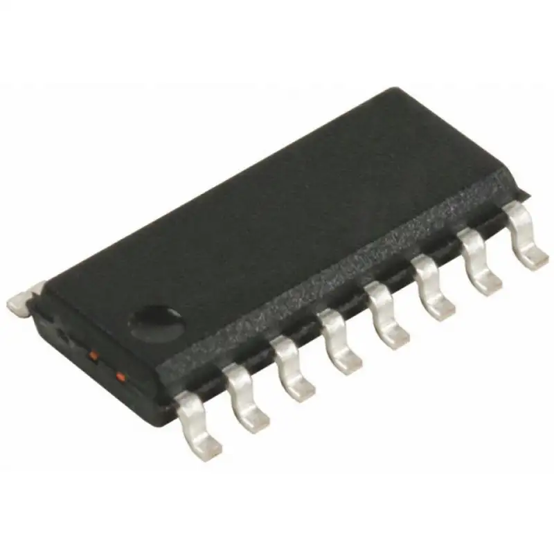
- CD4052 IC - (SMD Package) - Differential 4-channel Multiplexer/Demultiplexer IC
Click Image to Preview
CD4052 IC - (SMD Package) - Differential 4-channel Multiplexer/Demultiplexer IC
Brand: Generic | SKU: 1550963
₹ 19.48
₹ 29.73
Enter your pincode to check delivery options
Offer & Other Details
- Partial COD: Pay 30% Advance now and Balance on Delivery (COD).
- COD order value minimum Rs 600.
- Sales Assistance: Contact us +91 7358308283 for personalized advice.
Description
The CD4052 analog multiplexers/demultiplexers are digitally controlled analog switches having low “ON†impedance and very low “OFF†leakage currents. Control of analog signals up to 15Vp-p can be achieved by digital signal amplitudes of 3−15V. For example, if VDD = 5V, VSS = 0V and VEE = −5V, analog signals from −5V to +5V can be controlled by digital inputs of 0−5V. The multiplexer circuits dissipate extremely low quiescent power over the full VDD−VSS and VDD−VEE supply voltage ranges, independent of the logic state of the control signals. When a logical “1†is present at the inhibit input terminal all channels are “OFFâ€. A, B, and C, and an inhibit input. The three binary signals select 1 of 8 channels to be turned “ON†and connect the input to the output. CD4052 is a differential 4-channel multiplexer having two binary control inputs, A and B, and an inhibit input.
Features:-
• Wide range of digital and analog signal levels: digital 3 – 15V, analog to 15Vp-p
• Low “ON†resistance: 80Ω (typ.) over entire 15Vp-p signal-input range for VDD − VEE = 15V
• High “OFF†resistance: channel leakage of ±10 pA (typ.) at VDD − VEE = 10V
• Logic level conversion for digital addressing signals of 3 – 15V (VDD − VSS = 3 – 15V) to switch analog signals to 15 Vp-p (VDD − VEE = 15V)
• Matched switch characteristics: ∆RON = 5Ω (typ.) for VDD − VEE = 15V
• Very low quiescent power dissipation under all digital-control input and supply conditions: 1 µ W (typ.) at VDD − VSS = VDD − VEE = 10V
• Binary address decoding on chip
Specification:-
| Symbol | Parameter | Values |
| VDD | DC Supply Voltage | −0.5 VDC to +18 VDC |
| VIN | Input Voltage | 0.5 VDC to VDD +0.5 VDC |
| TS | Storage Temperature | −65°C to +150°C |
| PD | Power Dissipation | 700 mW |
| TL | Lead Temperature | 260°C |
Related Document:-

Related Products


Product added to cart!

