- ICs
- Magnet
- MicroControllers
- PCB & Solder
-
Small Components
- Aluminium Heat Sink
- Capacitor
- Crystal
- Diodes
- Diodes and Rectifiers
- Fuse
- Fuse Fuse Holder
- General Diodes
- General Purpose Transistor
- Hardware Parts
- Heat Shrink
- Heat Shrink Tube
- Heat Sink
- IC Base Socket
- IC Base ZIF Sockets
- IGBT
- Inductor
- JFET
- LED
- MOSFET
- MOV Metal Oxide Varistor
- Operational Amplifier
- Optocoupler
- PCB Adapter
- Potentiometer
- Power Transistor
- PVC Heat Shrink
- Resistance
- Resistor
- Schottky Diode
- SCR Thyristor
- SMD Resistor Reel
- Speaker
- Splices
- Testing Instruments
- Thermistor
- Transistors
- TRIAC
- Triac Mosfet
- Zener Diode
- SMD Components
- Switches
- AC DC Board Adaptor
- Adapter
-
Battery
- Battery Chargers
- Battery Connector
- Battery Harness
- Battery Holder
- Battery Holder
- Battery Protection Board
- BMS
- Bonka Lipo Battery
- Button Cell Battery
- CNC and PLC Machine Battery
- Coin Cell Battery
- Hearing Aid Battery
- Lead Acid Battery
- Li Ion Battery
- Lipo Battery
- Mobile Battery
- Ni Mh Battery
- Ni-Cd Battery
- Non Rechargeable Battery
- Other Battery Products
- Rechargeable Battery
- Ultra Lithium Battery
- Buck Boost Converter
- Cooling Block
- Cooling Fan
- HI Link Converter
- Meanwell SMPS
- Mornsun Power Supply
- Power Supply Module
- Shavison SMPS & PowerSupply
- SMPS
- Solar Panel
- Transformer
- Voltage Regulators
- 3D Printer Couplings
- 3D Printer Display Controller
- 3D Printer Extruder Kit
- 3D Printer Extruder Part And Fan
- 3D Printer Heat Bed Accessories
- 3D Printer Nozzle
- 3D Printer Parts
- 3D Printing Pen
- Basic Robot Parts
- DC Motor
- DIY STEM Kit
- Drone
- Drone Parts
- Lead Screw and Nut
- Motor Accessories
- Motor Driver
- Motor Driver IC
- New Arrival
- Home
- Electronic Components
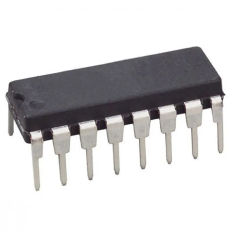
- CD40109 CMOS Quad Low-to-High Voltage Level Shifter IC DIP-16 Package

Click Image to Preview
CD40109 CMOS Quad Low-to-High Voltage Level Shifter IC DIP-16 Package
Brand: Generic | SKU: 2105260
₹ 60.48
₹ 79.95
Enter your pincode to check delivery options
Offer & Other Details
- Partial COD: Pay 30% Advance now and Balance on Delivery (COD).
- COD order value minimum Rs 600.
- Sales Assistance: Contact us +91 8903831010 for personalized advice.
Description
CD40109 contains four low-to-high-voltage level-shifting circuits. Each circuit will shift a low-voltage digital-logic input signal (A, B, C, D) with logical 1 = V CC and logical 0 = V SS to a high-voltage output signal (E, F, G, H) with logical 1 = V DD and logical 0 = V SS .
The RCA-CD40109, unlike other low-to-high level-shifting circuits, does not require the presence of the high-voltage supply (V DD ) before the application of either the low-voltage supply (V CC ) or the input signals. There are no restrictions on the sequence of application of V DD , V CC , or the input signals. In addition, with one exception there are no restrictions on the relative magnitudes of the supply voltages or input signals within the device maximum ratings, provided that the input signal swings between V SS and at least 0.7 V CC ; V CC may exceed V DD , and input signals may exceed V CC and V DD . When operated in the mode V CC > V DD , the CD40109 will operate as a high-to-low level-shifter.
The CD40109 also features individual three-state output capability. A low level on any of the separately enabled three-state output controls produces a high-impedance state in the corresponding output.
Features:-
- Qualified for Automotive Applications
-
Independent of Power Supply Sequence Considerations
- V CC Can Exceed V DD
- Input Signals can Exceed Both V CC and V DD
- Up and Down Level-Shifting Capability
- Three-State Outputs With Separate Enable Controls
- Standardized Symmetrical Output Characteristics
- 100% Tested for Quiescent Current at 20Â V
-
Maximum Input Current:
- 1 µA at 18 V Over Full Package-Temperature Range
- 100 nA at 18 V and 25°C
-
Noise Margin (Full Package-Temperature Range):
- 1 V at V CC = 5 V, V DD = 10 V
- 2 V at V CC = 10 V, V DD = 15 V
- 5-V, 10-V, and 15-V Parametric Ratings
- Meets All Requirements of JEDEC Tentative Standard No. 13B, "Standard specifications for Description of ’B’ Series CMOS Devices"
- Latch-Up Performance Meets 50 mA per JESD 78, Class I
-
APPLICATIONS
- High-or-Low Level-Shifting With Three-State Outputs for Unidirectional or Bidirectional Bussing
- Isolation of Logic Subsystem Using Separate Power Supplies from Supply Sequencing, Supply Loss, and Supply Regulation Considerations.
Specifications:-
| Parameters | Specification |
| Part number | CD40109B-Q1 |
| Technology Family | CD4000 |
| Bits (#) | 4 |
| Voltage (Nom) (V) | 5, 10, 15 |
| IOH (Max) (mA) | -6.8 |
| IOL(Max)(mA) | 6.8 |
| F @ nom voltage (Max) (MHz) | 50 |
| ICC @ nom voltage (Max) Â (mA) | 0.001 |
| Schmitt trigger | No |
| tpd @ nom Voltage (Max) (ns) | 600 |
| Rating | See Datasheet |
| Package Group | SO | 16 |
Related Documents:-
Related Products
Product added to cart!


