- ICs
- Magnet
- MicroControllers
- PCB & Solder
-
Small Components
- Aluminium Heat Sink
- Capacitor
- Crystal
- Diodes
- Diodes and Rectifiers
- Fuse
- Fuse Fuse Holder
- General Diodes
- General Purpose Transistor
- Hardware Parts
- Heat Shrink
- Heat Shrink Tube
- Heat Sink
- IC Base Socket
- IC Base ZIF Sockets
- IGBT
- Inductor
- JFET
- LED
- MOSFET
- MOV Metal Oxide Varistor
- Operational Amplifier
- Optocoupler
- PCB Adapter
- Potentiometer
- Power Transistor
- PVC Heat Shrink
- Resistance
- Resistor
- Schottky Diode
- SCR Thyristor
- SMD Resistor Reel
- Speaker
- Splices
- Testing Instruments
- Thermistor
- Transistors
- TRIAC
- Triac Mosfet
- Zener Diode
- SMD Components
- Switches
- AC DC Board Adaptor
- Adapter
-
Battery
- Battery Chargers
- Battery Connector
- Battery Harness
- Battery Holder
- Battery Holder
- Battery Protection Board
- BMS
- Bonka Lipo Battery
- Button Cell Battery
- CNC and PLC Machine Battery
- Coin Cell Battery
- Hearing Aid Battery
- Lead Acid Battery
- Li Ion Battery
- Lipo Battery
- Mobile Battery
- Ni Mh Battery
- Ni-Cd Battery
- Non Rechargeable Battery
- Other Battery Products
- Rechargeable Battery
- Ultra Lithium Battery
- Buck Boost Converter
- Cooling Block
- Cooling Fan
- HI Link Converter
- Meanwell SMPS
- Mornsun Power Supply
- Power Supply Module
- Shavison SMPS & PowerSupply
- SMPS
- Solar Panel
- Transformer
- Voltage Regulators
- 3D Printer Couplings
- 3D Printer Display Controller
- 3D Printer Extruder Kit
- 3D Printer Extruder Part And Fan
- 3D Printer Heat Bed Accessories
- 3D Printer Nozzle
- 3D Printer Parts
- 3D Printing Pen
- Basic Robot Parts
- DC Motor
- DIY STEM Kit
- Drone
- Drone Parts
- Lead Screw and Nut
- Motor Accessories
- Motor Driver
- Motor Driver IC
- New Arrival
- Home
- Integrated Circuits
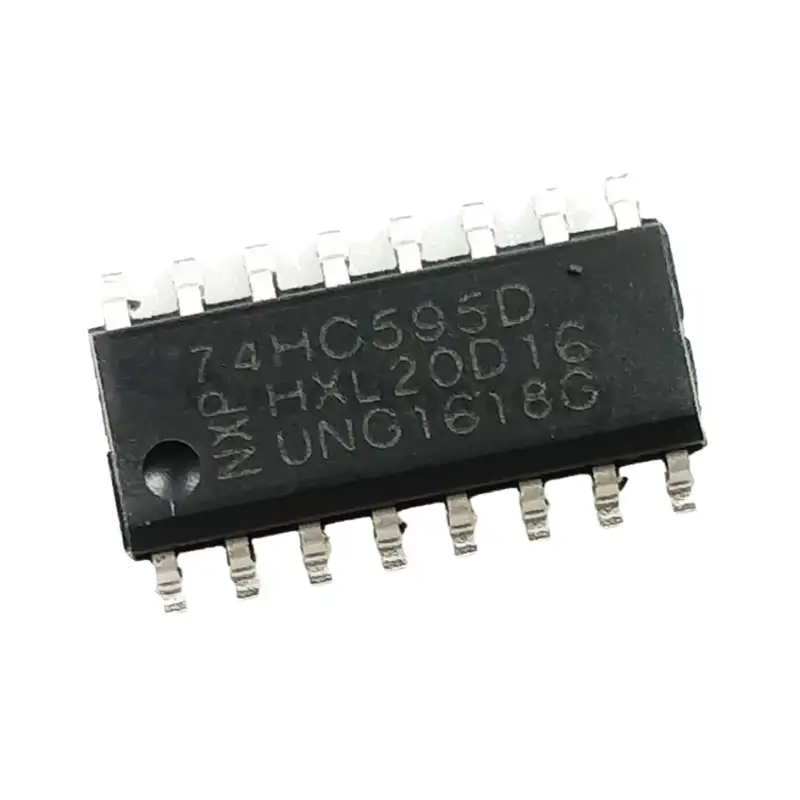
- 74HC595 8-bit serial-in, serial or parallel-out shift register with output latches; 3-state

Click Image to Preview
74HC595 8-bit serial-in, serial or parallel-out shift register with output latches; 3-state
Brand: Generic | SKU: 3155869
₹ 11.00
₹ 14.00
Enter your pincode to check delivery options
Offer & Other Details
- Payment Offer: 2% Instant Discount on UPI and bank Transfer Payments.
- Partial COD: Pay 25% Advance now and Balance on Delivery (COD).
- Sales Assistance: Contact us +91 8903831010 for personalized advice.
Description
The 74HC595 are high-speed Si-gate CMOS devices and are pin-compatible with low power Schottky TTL (LSTTL). They are specified in compliance with JEDEC.The 74HC595 is an 8-stage serial shift register with a storage register and 3-state outputs. The shift register and storage register have separate clocks. Data is shifted on the positive-going transitions of the SH_CP input. The data in each register is transferred to the storage register on a positive-going transition of the ST_CP input. If both clocks are connected together, the shift register will always be one clock pulse ahead of the storage register.The shift register has a serial input (DS) and a serial standard output (Q7’) for cascading. It is also provided with asynchronous reset (active LOW) for all 8 shift register stages. The storage register has 8 parallel 3-state bus driver outputs. Data in the storage register appears at the output whenever the output enable input (OE) is LOW.
Pin Configuration
Pin Number
Pin Name
Description
1,2,3,4,5,6,7
Output Pins (Q1 to Q7)
parallel data output
8
Ground
Connected to the Ground of the circuit
9
Q7
serial data output
10
(MR) Master Reset
master reset (active LOW)
11
(SH_CP) Clock
This is the clock pin to which the clock signal has to be provided from MCU/MPU
12
(ST_CP) Latch
The Latch pin is used to update the data to the output pins. It is active high
13
(OE) Output Enable
The Output Enable is used to turn off the outputs. Must be held low for normal operation
14
(DS) Serial Data
This is the pin to which data is sent, based on which the 8 outputs are controlled
15
(Q0) Output
The first output pin.
16
Vcc
This pin powers the IC, typically +5V is used.
FEATURES
APPLICATIONS
Supply voltage
2 - 6V
TEMPERATURE RANGE
−40°C to +125°C
Pins
16
Package
SO16
Ambient temperature
−40°C ~ +125°C
Dimensions
10mm x 6mm x 1.6mm
Related Products
Product added to cart!

